7
There may be a second restriction on the size of the
resistors used to set the linear regulators output voltage
based on ACPI functionality. Read the ACPI
Implementation section under Application Guidelines to
see if this additional constraint concerns your application. To
ensure the parallel combination of the feedback resistors
equals a certain chosen value, R
FB
, use the following
equations:
, where
V
OUT
- the desired output voltage,
V
FB
- feedback (reference) voltage, 0.8V.
Application Guidelines
Soft-Start Interval
The soft-start function controls the output voltages rate of rise
to limit the current surge at start-up. The soft-start function is
integrated on the chip and the soft-start interval is thus fixed.
Layout Considerations
MOSFETs switch very fast and efficiently. The speed with
which the current transitions from one device to another
causes voltage spikes across the interconnecting
impedances and parasitic circuit elements. The voltage
spikes can degrade efficiency, radiate noise into the circuit,
and lead to device overvoltage stress. Careful component
layout and printed circuit design minimizes the voltage
spikes in the converter. Consider, as an example, the turn-
off transition of the upper PWM MOSFET. Prior to turn-off,
the upper MOSFET was carrying the full load current.
During the turn-off, current stops flowing in the upper
MOSFET and is picked up by the lower MOSFET or
Schottky diode. Any inductance in the switched current
path generates a large voltage spike during the switching
interval. Careful component selection, tight layout of the
critical components, and short, wide circuit traces minimize
the magnitude of voltage spikes.
There are two sets of critical components in a DC-DC
converter using a ISL6432 controller. The switching power
components are the most critical because they switch large
amounts of energy, and as such, they tend to generate
equally large amounts of noise. The critical small signal
components are those connected to sensitive nodes or
those supplying critical bypass current.
The power components and the controller IC should be
placed first. Locate the input capacitors, especially the high-
frequency ceramic decoupling capacitors, close to the power
switches. Locate the output inductor and output capacitors
between the MOSFETs and the load. Locate the PWM
controller close to the MOSFETs.
The critical small signal components include the bypass
capacitor for VCC and the feedback resistors. Locate these
components close to their connecting pins on the control IC.
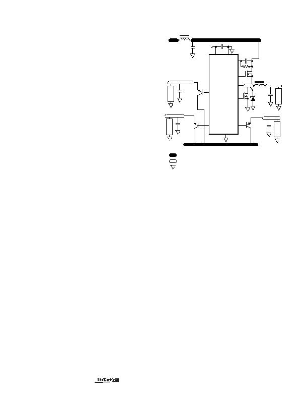
A multi-layer printed circuit board is recommended. Figure 4
shows the connections of the critical components in the
converter. Note that the capacitors C
IN
and C
OUT
each
represent numerous physical capacitors. Dedicate one solid
layer for a ground plane and make all critical component
ground connections with vias to this layer. Dedicate another
solid layer as a power plane and break this plane into smaller
islands of common voltage levels. The power plane should
support the input power and output power nodes. Use copper
filled polygons on the top and bottom circuit layers for the
PHASE nodes, but do not unnecessarily oversize these
particular islands. Since the PHASE nodes are subjected to
very high dV/dt voltages, the stray capacitor formed between
these islands and the surrounding circuitry will tend to couple
switching noise. Use the remaining printed circuit layers for
small signal wiring. The wiring traces from the control IC to the
MOSFET gate and source should be sized to carry 2A peak
currents.
PWM Controller Feedback Compensation
The PWM controller uses voltage-mode control for output
regulation. This section highlights the design consideration
for a PWM voltage-mode controller. Apply the methods and
considerations only to the PWM controller.
Figure 5 highlights the voltage-mode control loop for a
synchronous-rectified buck converter. The output voltage
(V
OUT
) is regulated to the Reference voltage level, 0.8V. The
R
S
V
OUT
V
FB
--------------- - R
FB
?/DIV>
=
R
P
R
S
V
FB
?/DIV>
V
OUT
V
FB
-------------------------------- -
=
FIGURE 4. PRINTED CIRCUIT BOARD POWER PLANES AND
ISLANDS
V
OUT1
Q1
Q2
Q3
Q4
+12V
C
VCC
VIA CONNECTION TO GROUND PLANE
ISLAND ON POWER PLANE LAYER
ISLAND ON CIRCUIT OR POWER PLANE LAYER
L
OUT
C
OUT1
CR1
ISL6432
C
IN
C
OUT2
V
OUT2
V
OUT3
+5V
IN
PGND
LGATE
UGATE
PHASE
DRIVE3
KEY
GND
VCC
DRIVE2
OCSET
R
OCSET
C
OCSET
V
OUT4
DRIVE4
+3.3V
IN
L
IN
Q5
C
OUT3
C
OUT4
+
+
+
+
+
ISL6432
发布紧急采购,3分钟左右您将得到回复。
相关PDF资料
ISL6521CBZS2698
IC REG QD BCK/LINEAR 16-SOIC
ISL6528CBZ-TS2698
IC REG DL BCK/LINEAR SYNC 8-SOIC
ISL6529CBZ
IC REG DL BCK/LINEAR SYNC 14SOIC
ISL6534CVZ-TR5229
IC REG 3OUT BCK/LINEAR 24EPTSSOP
ISL6549CRZR5213
IC REG DL BCK/LINEAR SYNC 16-QFN
ISL9305IRTHWLNCZ-T
IC REG QD BUCK/LINEAR 16TQFN
ISL9305IRTWLNCZ-T
IC REG QD BUCK/LINEAR 16TQFN
ISL9307IRTWCWNZ-T
IC REG QD BCK/LINEAR SYNC 16TQFN
相关代理商/技术参数
ISL6433BCB
制造商:Intersil Corporation 功能描述:
ISL6434CB
制造商:Intersil Corporation 功能描述:
ISL6435CA
制造商:Intersil Corporation 功能描述:
ISL6436HIB
制造商:Intersil Corporation 功能描述:
ISL6436LIB
功能描述:IC CTRLR PS USB DUAL PORT 8-SOIC RoHS:否 类别:集成电路 (IC) >> 接口 - 控制器 系列:- 标准包装:4,900 系列:- 控制器类型:USB 2.0 控制器 接口:串行 电源电压:3 V ~ 3.6 V 电流 - 电源:135mA 工作温度:0°C ~ 70°C 安装类型:表面贴装 封装/外壳:36-VFQFN 裸露焊盘 供应商设备封装:36-QFN(6x6) 包装:* 其它名称:Q6396337A
ISL6439ACB
制造商:Rochester Electronics LLC 功能描述:- Bulk 制造商:Intersil Corporation 功能描述:
ISL6439ACB-T
制造商:Rochester Electronics LLC 功能描述:- Bulk 制造商:Intersil Corporation 功能描述:
ISL6439ACR
制造商:Rochester Electronics LLC 功能描述:- Bulk 制造商:Intersil Corporation 功能描述: